
- 非IC关键词
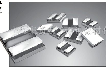
企业档案
- 相关证件:

- 会员类型:普通会员
- 白卫平

- 电话:029-88221540
- 手机:13720772046
- 地址:西安市雁塔区太白南路263号
- 传真:029-88221540
- E-mail:baiweiping@365-24.com.cn
产品分类
您的当前位置:上海集新电子通讯器材有限公司 > 元器件产品
产品信息
Sales and Corporate Office
1717 Chicago Avenue
Riverside, California 92507-2364
Phone: (951) 788-1700
Fax: (951) 369-1151
Applications Engineering
17271 North Umpqua Hwy.
Roseburg, Oregon 97470-9422
Phone: (541) 496-0700
Fax: (541) 496-0408
© 2003-2007 Caddock Electronics, Inc. CADDOCK e-mail: • web: www.caddock.com
For Caddock Distributors listed by country see caddock.com/contact/dist.html
ELE*RONICS, INC.
28_IL117.1004
CD2015FC Standard Resistance Values:
Tolerance CD2015FC ±1% Standard.
CD2520FC Standard Resistance Values:
0.010 Ω
0.015 Ω
0.020 Ω
0.025 Ω
Tolerance CD2520FC ±1% Standard.
0.030 Ω
0.033 Ω
0.040 Ω
0.050 Ω
0.075 Ω
0.10 Ω
0.20 Ω
Custom resistance values and non-standard tolerances
can be manufactured for high quantity applications.
Please contact Caddock Applications Engineering.
Recommended Circuit Board Layout
(current and sense connections):
Fig. 1A: Recommended Kelvin layout.
0.010 Ω 0.20 Ω
Model
Resistance
Min. Max.
Power Capability Information
CD2015FC
CD2520FC 0.010 Ω 0.20 Ω
1.0 Watt 150°C
Max. Chip
Temperature
General Applications High Power Applications
Thermal Resistance - RθJC
Film (J) to Solder Pad (C)
(see note 2)
12.0°C/Watt
Power Rating
at 70° C
(see note 1)
9.0°C/Watt 150°C
Dimensions in inches and (millimeters)
.200 ±.012
(5.08 ±.30
A B D
.150 ±.012
(3.81 ±.30)
.062 min.
(1.57 min.)
C
.063 ±.006
(1.60 ±.15)
.250 ±.012
(6.35 ±.30)
.200 ±.012
(5.08 ±.30)
.078 min.
(1.98 min.)
.063 ±.006
(1.60 ±.15
Comments
Solderable Pedestal
1.5 Watts Solderable Pedestal
T*e CD Low Resistance Precision Chip Resistors
Style FC - Flip Chip Version is a surface mount version with solderable pedestal terminals for flip chip soldering.
Note 1: General Applications - The power rating for
general applications is based upon 0.5 sq. in. (300
mm2) of termination pad or trace area (2 oz. copper)
connected to each end of the resistor. Maximum chip
temperature is 150°C. Use Derating Curve to derate
appropriay for the maximum ambient temperature
and for the temperature limitations of the adjacent
materials.
Note 2: Thermal Resistance - In High Power Applications where the circuit board material
provides high heat sinking benefits (such as IMS, Alumina, or other) the thermal resistance of
the chip resistor is useful to establish the maximum power capability of the chip resistor in the
application. The film temperature is measured at the center of the resistor element and solder
pad temperature at the center of the solderable pedestal (point X in the recommended circuit
layout shown below). Maximum temperature of the chip resistor (at the center of chip) should
not exceed 150°C through the temperature range of the application.
Style FC Derating Curve For General Applications
A*ENT TEMPERATURE, C
RATED LOAD, %
o
100
80
60
40
20
0
250
C = Current connection
S = Sense connection
Note: Actual width of current trace is based on
magnitude of current. Point of connection should
be in the area shown.
Low Resistance Chip down to 0.010Ω at ±1% with unique Pedestal Terminal Design
for Current Sense in Hybrid and SMT Applications
0.010 Ω
0.015 Ω
0.020 Ω
0.025 Ω
0.030 Ω
0.033 Ω
0.040 Ω
0.050 Ω
0.075 Ω
0.10 Ω
0.20 Ω
S S
X X
C C
T*e CD Low Resistance Precision Chip Resistors utilize the proven Caddock
Micronox® resistance films to achieve the unique low resistance range in this
family. The special performance features of the T*e CD Low Resistance
Precision Film Resistor include:
• Style FC - Flip Chip version for surface mount applications.
Style WB - Wire Bond version for hybrid applications with metallized
back surface for solder down heat sinking of the chip, includes bondable
termination pedestals to receive aluminum wire bonds.
• Resistance as low as 0.010 ohm at ±1%.
• Pedestal terminals in this design provide an ultra low resistance
connection pad which maintains the precision 0.010Ω ±1% at the point
of customer Kelvin connection to the resistor chip. The pedestal terminal
with its copper core also provides heat spreading which enhances the
high power handling capability.
• Thermal resistance is provided to optimize high power designs when
utilizing higher thermal conductivity circuit board substrates such as IMS
or Alumina.
• High pulse handling and overload capability.
• Low inductance provides excellent high frequency and pulse response.
Page 1 of 2
Sales and Corporate Office
1717 Chicago Avenue
Riverside, California 92507-2364
Phone: (951) 788-1700
Fax: (951) 369-1151
Applications Engineering
17271 North Umpqua Hwy.
Roseburg, Oregon 97470-9422
Phone: (541) 496-0700
Fax: (541) 496-0408
e-mail: • web: www.caddock.com
For Caddock Distributors listed by country see caddock.com/contact/dist.html
© 2003-2007 Caddock Electronics, Inc.
ELE*RONICS, INC.
28_IL117.1004
is a hybrid mountable version with copper pedestal terminals and an aluminum surface layer for wire
bonding. The back surface of these devices is metallized for solder attachment of the chip resistor to a heat sinking substrate.
Specifications:
Temperature Coefficient: TC referenced to
+25°C, ΔR taken at +150°C.
0.050 ohm to 0.20 ohm, 0 to +100 ppm/°C.
0.010 ohm to 0.049 ohm, 0 to +200 ppm/°C.
Inductance: Less than 5 nH t*ical.
Load Life: 1000 hours at rated power, based
upon 150°C max. chip temperature,
ΔR ± (0.5% + 0.0005 ohm).
Momentary Overload: 1.5 times rated
power, for 5 seconds, ΔR ± (0.5% + 0.0005
ohm).
Operating Temperature: -55°C to +150°C.
Measurement Note: All measurements
are taken using Kelvin connections per the
recommended connection locations.
Ordering
Information:
Ko signifies tape thickness and dimension
12mm
0.473”
Ao
Bo
7” dia.
(178 mm)
.512” arbor hole
(13mm)
Packaging information:
Style FC, flip chip resistors, are shipped with the bare
ceramic side up in the pocket, with the solderable pedestals
facing down.
Style WB, wire bondable resistors, are shipped with the
wire bondable pedestals facing up in the pocket.
The illustration shows the orientation of the CD2015 chip
resistors in the tape. The CD2520 chip resistors are rotated 90°
from what is shown in the illustration.
Style WB - Wire Bond Version
Note 3: Thermal Resistance - In High Power Applications where the circuit board material
provides high heat sinking benefits (such as IMS, Alumina, or other) the thermal resistance of
the chip resistor is useful to establish the maximum power capability of the chip resistor in the
application. The film temperature is measured at the center of the resistor element and the
solder pad temperature is measured at the soldered interface with the circuit board. Maximum
temperature of the chip resistor (at the center of chip) should not exceed 150°C through the
temperature range of the application.
WB Resistor mounting
Circuit board: IMS, Ceramic (Alumina) , or other.
Sense Wire
Current Wire
Film Temperature
Measuring Point
Solder pad, soldered
interface with circuit board.
Sense Wire
Current Wire
Location for Sense (Potential) Connection:
General Information for T*e CD - Style FC and Style WB - Chip Resistors
Solder attachment notes:
During soldering of the T*e CD Resistor
the soldering temperature profile must not
cause the pedestal terminals of this device
to exceed 220°C.
Style FC - Flip Chip version resistors
have a bare ceramic back surface. The
recommended solder for flip chip solder
attachment is 62Sn / 36Pb / 2Ag.
Style WB - Wire Bond version resistors
have a metallized back surface for
soldering to a substrate or a heat sink.
The recommended solder is
62Sn / 36Pb / 2Ag.
Model
Resistance
Min. Max.
Power Capability Information
Max. Chip
Temperature
Thermal Resistance
RθJC
Film (J) to Solder Pad (C)
(see note 3)
Dimensions in inches and (millimeters)
A B C D
Comments
8.33°C/Watt 150°C .200 ±.012
(5.08 ±.30)
.150 ±.012
(3.81 ±.30)
.062 min.
(1.57 min.)
.061 ±.005
(1.55 ±.13)
Terminals have an Aluminum surface layer for
CD2015WBA 0.010 Ω 0.20 Ω wire bonding. Aluminum wire to be used for bonding.
CD2520WBA 0.010 Ω 0.20 Ω 5.00°C/Watt 150°C .250 ±.012
(6.35 ±.30)
.200 ±.012
(5.08 ±.30)
.078 min.
(1.98 min.)
.061 ±.005
(1.55 ±.13)
Terminals have an Aluminum surface layer for
wire bonding. Aluminum wire to be used for bonding.
Custom resistance values and non-standard tolerances
can be manufactured for high quantity applications.
Please contact Caddock Applications Engineering.
CD 2520 FC - 0.10 - 1%
T*e CD
Physical Size
2015 = 0.200” x 0.150”
2520 = 0.250” x 0.200”
Style:
FC or WBA
Resistor Value (Ω)
See charts for availability
Tolerance:
±1% 0.010 Ω and above.
Full reel quantities:
1000 pieces per reel for CD2015 and CD2520
Quantities of less than 250 will be shipped in tape without reel
and without tape leader at the option of Caddock.
Tape dimensions and materials will be consistent with EIA-481-1.
Reels will be marked with a label containing Caddock logo, part
Dimensions in inches and (millimeters) number, resistor value, tolerance, packaging date, and quantity.
D
A
B
C
Carrier Tape and pocket dimensions:
Tape is 12mm Carrier Tape (8mm pitch)
0.189” (4.80mm)
Size 2015
0.209” (5.31mm)
0.087” (2.21mm)
0.271” (6.88mm)
Size 2520
0.216” (5.49mm)
0.066” (1.68mm)
Ao
Bo
Ko
Note: The sense connection for each
pedestal is positioned inboard of the current
connection (single or multiple current wires).
Tolerance CD2015WBA ±1% Standard.
CD2015WBA
Standard Resistance Values:
0.010 Ω
0.015 Ω
0.020 Ω
0.025 Ω
0.030 Ω
0.033 Ω
0.040 Ω
0.050 Ω
0.075 Ω
0.10 Ω
0.20 Ω
Tolerance CD2520WBA ±1% Standard.
CD2520WBA
Standard Resistance Values:
0.010 Ω
0.015 Ω
0.020 Ω
0.025 Ω
0.030 Ω
0.033 Ω
0.040 Ω
0.050 Ω
0.075 Ω
0.10 Ω
0.20 Ω
T*e CD Low Resistance Precision Chip Resistors
Page 2 of 2
1717 Chicago Avenue
Riverside, California 92507-2364
Phone: (951) 788-1700
Fax: (951) 369-1151
Applications Engineering
17271 North Umpqua Hwy.
Roseburg, Oregon 97470-9422
Phone: (541) 496-0700
Fax: (541) 496-0408
© 2003-2007 Caddock Electronics, Inc. CADDOCK e-mail: • web: www.caddock.com
For Caddock Distributors listed by country see caddock.com/contact/dist.html
ELE*RONICS, INC.
28_IL117.1004
CD2015FC Standard Resistance Values:
Tolerance CD2015FC ±1% Standard.
CD2520FC Standard Resistance Values:
0.010 Ω
0.015 Ω
0.020 Ω
0.025 Ω
Tolerance CD2520FC ±1% Standard.
0.030 Ω
0.033 Ω
0.040 Ω
0.050 Ω
0.075 Ω
0.10 Ω
0.20 Ω
Custom resistance values and non-standard tolerances
can be manufactured for high quantity applications.
Please contact Caddock Applications Engineering.
Recommended Circuit Board Layout
(current and sense connections):
Fig. 1A: Recommended Kelvin layout.
0.010 Ω 0.20 Ω
Model
Resistance
Min. Max.
Power Capability Information
CD2015FC
CD2520FC 0.010 Ω 0.20 Ω
1.0 Watt 150°C
Max. Chip
Temperature
General Applications High Power Applications
Thermal Resistance - RθJC
Film (J) to Solder Pad (C)
(see note 2)
12.0°C/Watt
Power Rating
at 70° C
(see note 1)
9.0°C/Watt 150°C
Dimensions in inches and (millimeters)
.200 ±.012
(5.08 ±.30
A B D
.150 ±.012
(3.81 ±.30)
.062 min.
(1.57 min.)
C
.063 ±.006
(1.60 ±.15)
.250 ±.012
(6.35 ±.30)
.200 ±.012
(5.08 ±.30)
.078 min.
(1.98 min.)
.063 ±.006
(1.60 ±.15
Comments
Solderable Pedestal
1.5 Watts Solderable Pedestal
T*e CD Low Resistance Precision Chip Resistors
Style FC - Flip Chip Version is a surface mount version with solderable pedestal terminals for flip chip soldering.
Note 1: General Applications - The power rating for
general applications is based upon 0.5 sq. in. (300
mm2) of termination pad or trace area (2 oz. copper)
connected to each end of the resistor. Maximum chip
temperature is 150°C. Use Derating Curve to derate
appropriay for the maximum ambient temperature
and for the temperature limitations of the adjacent
materials.
Note 2: Thermal Resistance - In High Power Applications where the circuit board material
provides high heat sinking benefits (such as IMS, Alumina, or other) the thermal resistance of
the chip resistor is useful to establish the maximum power capability of the chip resistor in the
application. The film temperature is measured at the center of the resistor element and solder
pad temperature at the center of the solderable pedestal (point X in the recommended circuit
layout shown below). Maximum temperature of the chip resistor (at the center of chip) should
not exceed 150°C through the temperature range of the application.
Style FC Derating Curve For General Applications
A*ENT TEMPERATURE, C
RATED LOAD, %
o
100
80
60
40
20
0
250
C = Current connection
S = Sense connection
Note: Actual width of current trace is based on
magnitude of current. Point of connection should
be in the area shown.
Low Resistance Chip down to 0.010Ω at ±1% with unique Pedestal Terminal Design
for Current Sense in Hybrid and SMT Applications
0.010 Ω
0.015 Ω
0.020 Ω
0.025 Ω
0.030 Ω
0.033 Ω
0.040 Ω
0.050 Ω
0.075 Ω
0.10 Ω
0.20 Ω
S S
X X
C C
T*e CD Low Resistance Precision Chip Resistors utilize the proven Caddock
Micronox® resistance films to achieve the unique low resistance range in this
family. The special performance features of the T*e CD Low Resistance
Precision Film Resistor include:
• Style FC - Flip Chip version for surface mount applications.
Style WB - Wire Bond version for hybrid applications with metallized
back surface for solder down heat sinking of the chip, includes bondable
termination pedestals to receive aluminum wire bonds.
• Resistance as low as 0.010 ohm at ±1%.
• Pedestal terminals in this design provide an ultra low resistance
connection pad which maintains the precision 0.010Ω ±1% at the point
of customer Kelvin connection to the resistor chip. The pedestal terminal
with its copper core also provides heat spreading which enhances the
high power handling capability.
• Thermal resistance is provided to optimize high power designs when
utilizing higher thermal conductivity circuit board substrates such as IMS
or Alumina.
• High pulse handling and overload capability.
• Low inductance provides excellent high frequency and pulse response.
Page 1 of 2
Sales and Corporate Office
1717 Chicago Avenue
Riverside, California 92507-2364
Phone: (951) 788-1700
Fax: (951) 369-1151
Applications Engineering
17271 North Umpqua Hwy.
Roseburg, Oregon 97470-9422
Phone: (541) 496-0700
Fax: (541) 496-0408
e-mail: • web: www.caddock.com
For Caddock Distributors listed by country see caddock.com/contact/dist.html
© 2003-2007 Caddock Electronics, Inc.
ELE*RONICS, INC.
28_IL117.1004
is a hybrid mountable version with copper pedestal terminals and an aluminum surface layer for wire
bonding. The back surface of these devices is metallized for solder attachment of the chip resistor to a heat sinking substrate.
Specifications:
Temperature Coefficient: TC referenced to
+25°C, ΔR taken at +150°C.
0.050 ohm to 0.20 ohm, 0 to +100 ppm/°C.
0.010 ohm to 0.049 ohm, 0 to +200 ppm/°C.
Inductance: Less than 5 nH t*ical.
Load Life: 1000 hours at rated power, based
upon 150°C max. chip temperature,
ΔR ± (0.5% + 0.0005 ohm).
Momentary Overload: 1.5 times rated
power, for 5 seconds, ΔR ± (0.5% + 0.0005
ohm).
Operating Temperature: -55°C to +150°C.
Measurement Note: All measurements
are taken using Kelvin connections per the
recommended connection locations.
Ordering
Information:
Ko signifies tape thickness and dimension
12mm
0.473”
Ao
Bo
7” dia.
(178 mm)
.512” arbor hole
(13mm)
Packaging information:
Style FC, flip chip resistors, are shipped with the bare
ceramic side up in the pocket, with the solderable pedestals
facing down.
Style WB, wire bondable resistors, are shipped with the
wire bondable pedestals facing up in the pocket.
The illustration shows the orientation of the CD2015 chip
resistors in the tape. The CD2520 chip resistors are rotated 90°
from what is shown in the illustration.
Style WB - Wire Bond Version
Note 3: Thermal Resistance - In High Power Applications where the circuit board material
provides high heat sinking benefits (such as IMS, Alumina, or other) the thermal resistance of
the chip resistor is useful to establish the maximum power capability of the chip resistor in the
application. The film temperature is measured at the center of the resistor element and the
solder pad temperature is measured at the soldered interface with the circuit board. Maximum
temperature of the chip resistor (at the center of chip) should not exceed 150°C through the
temperature range of the application.
WB Resistor mounting
Circuit board: IMS, Ceramic (Alumina) , or other.
Sense Wire
Current Wire
Film Temperature
Measuring Point
Solder pad, soldered
interface with circuit board.
Sense Wire
Current Wire
Location for Sense (Potential) Connection:
General Information for T*e CD - Style FC and Style WB - Chip Resistors
Solder attachment notes:
During soldering of the T*e CD Resistor
the soldering temperature profile must not
cause the pedestal terminals of this device
to exceed 220°C.
Style FC - Flip Chip version resistors
have a bare ceramic back surface. The
recommended solder for flip chip solder
attachment is 62Sn / 36Pb / 2Ag.
Style WB - Wire Bond version resistors
have a metallized back surface for
soldering to a substrate or a heat sink.
The recommended solder is
62Sn / 36Pb / 2Ag.
Model
Resistance
Min. Max.
Power Capability Information
Max. Chip
Temperature
Thermal Resistance
RθJC
Film (J) to Solder Pad (C)
(see note 3)
Dimensions in inches and (millimeters)
A B C D
Comments
8.33°C/Watt 150°C .200 ±.012
(5.08 ±.30)
.150 ±.012
(3.81 ±.30)
.062 min.
(1.57 min.)
.061 ±.005
(1.55 ±.13)
Terminals have an Aluminum surface layer for
CD2015WBA 0.010 Ω 0.20 Ω wire bonding. Aluminum wire to be used for bonding.
CD2520WBA 0.010 Ω 0.20 Ω 5.00°C/Watt 150°C .250 ±.012
(6.35 ±.30)
.200 ±.012
(5.08 ±.30)
.078 min.
(1.98 min.)
.061 ±.005
(1.55 ±.13)
Terminals have an Aluminum surface layer for
wire bonding. Aluminum wire to be used for bonding.
Custom resistance values and non-standard tolerances
can be manufactured for high quantity applications.
Please contact Caddock Applications Engineering.
CD 2520 FC - 0.10 - 1%
T*e CD
Physical Size
2015 = 0.200” x 0.150”
2520 = 0.250” x 0.200”
Style:
FC or WBA
Resistor Value (Ω)
See charts for availability
Tolerance:
±1% 0.010 Ω and above.
Full reel quantities:
1000 pieces per reel for CD2015 and CD2520
Quantities of less than 250 will be shipped in tape without reel
and without tape leader at the option of Caddock.
Tape dimensions and materials will be consistent with EIA-481-1.
Reels will be marked with a label containing Caddock logo, part
Dimensions in inches and (millimeters) number, resistor value, tolerance, packaging date, and quantity.
D
A
B
C
Carrier Tape and pocket dimensions:
Tape is 12mm Carrier Tape (8mm pitch)
0.189” (4.80mm)
Size 2015
0.209” (5.31mm)
0.087” (2.21mm)
0.271” (6.88mm)
Size 2520
0.216” (5.49mm)
0.066” (1.68mm)
Ao
Bo
Ko
Note: The sense connection for each
pedestal is positioned inboard of the current
connection (single or multiple current wires).
Tolerance CD2015WBA ±1% Standard.
CD2015WBA
Standard Resistance Values:
0.010 Ω
0.015 Ω
0.020 Ω
0.025 Ω
0.030 Ω
0.033 Ω
0.040 Ω
0.050 Ω
0.075 Ω
0.10 Ω
0.20 Ω
Tolerance CD2520WBA ±1% Standard.
CD2520WBA
Standard Resistance Values:
0.010 Ω
0.015 Ω
0.020 Ω
0.025 Ω
0.030 Ω
0.033 Ω
0.040 Ω
0.050 Ω
0.075 Ω
0.10 Ω
0.20 Ω
T*e CD Low Resistance Precision Chip Resistors
Page 2 of 2